Constraint Posting for Verifying VLSI Circuits
Proceedings of the Eleventh International Joint Conference on Artificial Intelligence. Planning, Scheduling, Reasoning About Actions. Pages 881-885.
© 1989 International Joint Conferences on Artificial Intelligence
Abstract
We appl y constraint posting to the problem of reasoning about function from structure . Constraint posting is a technique used by some planners to coordinate decisions . At each decision point constraints are posted that later decisions must obey . We use constraint posting to help verify that a circuit modelled at the analog level will exhibit its intended digital behavior. A circuit 's analog behavior depends not only on the circuit 's structure , but also on how the circuit is used. We post constraints to ensure that a circuit will only be used commensurate with its intended function. This research shows that while there is no ''function from structure ," there is function from structure and constraint posting . We have implemented these ideas in program that rapidly verifies large circuits.
- [Barrow, 1985] Harry Barrow. Proving the correctness of hardware designs. VLSI Design, July 1984.
- [Davis, 1982] Randall Davis. Diagnosis based on de- scription of structure and function. Proceedings fo the National Conference on Artificial Intelligence , pages 137-142, Pittsburgh, PA, August 1982.
- [de Kleer, 1986] Johann de Kleer and Brian Williams. Reasoning about multiple faults. Proceedings of the National Conference on Artificial Intelligence, Pitts- [Mead/ Conway, 1980] Carver Mead and Lynn Conway. Introduction to VLSI Systems, Addison Wesley, 1980.
- [Minsky, 1963] Marvin Minsky. Steps towards artificial intelligence. Computers and Thought, Geigenbaum and Feldman, editors, McGraw-Hill, New York , 1963.
- [Nguyen, 1989] Tin Nguyen and Daniel Weise. Diagnos- ing Multiple Faults in Digital Systems. Fifth Annual IEEE Conference on AI Applications, Miami Beach, Florida, March 1989.
- [Stefik, 1981] Mark Stefik. Planning with constraints. Artificial Intelligence, 16(2):111-140, 1981.
- [Weise, 1986] Daniel Weise Formal Multilevel Hierarchi- cal Verification of Synchronous MOS VLSI Circuits. Technical Report AI-TR 978, Artificial Intelligence Laboratory, MIT, 1986.
References were extracted automatically from the PDF and may contain errors.
Full text extracted automatically from the PDF; figures, tables and equations may differ. The PDF is the version of record.
1 Introduction
Designers and planners deal with complexity by using hierarchical top down abstract planning [Minsky, 1963] . At each level of the planning/design hierarchy, a prob lem is solved by assuming ·an appropriate set of abstract high level operators and operands. The existence of the abstract operators and operands is proposed as subprob lems one level down in the planning/ design hierarchy, which are then solved to yield subplans. This process ends when t he original problem is solved solely in terms of primitive operands and operators. The achilles heel of this method is subproblem interaction: although the abstract subplans may compose at the abstract level to solve the initial problem, the actual primitives used to construct the abstract subplans may interfere and cause t he plan to fail.
Digital circuit designers use abstract planning to de sign large chips. They decompose a system into func tional units ( datapaths and control units), functional units into registers and logic, and registers and logic into t ransistors . The real primitives of design, namely resis tors , capacitors , and analog signals, are abstracted away at nearly every step. Simply put , designers treat inher ently non-digital components as digital. Very often a circuit is logically correct but rife with electrical prob lems.
·This research was sponsored by Darpa contracts N0001486-K-180 and N00014-85-K-0124 . The author was a Fannie and John Fellow when this research was conducted.
We use Constraint posting, a method first employed in Molgen [Stefik, 1981] to avoid subproblem interation, to verify that a circuit will exhibit its intended abstract (digital) behavior. The key idea is that subplans com municate via the physical entities of the plan. In Molgen these entities are bacteria, enzymes, vectors, and antibi otics. In circuit design the entities are analog signals: time varying continuously valued voltages and currents. Subplan interference manifests itself as the passing of inappropriate physical entities from subplan to subplan. This is because the primitive operators and operands that constitute a subplan prevent the subplan from work ing on all entities that it might be passed. Subproblem interference is avoided by having each decision post con straints on the inputs to the subplan the decision helps create, and then forcing subplans that create the entities passed to the subplan to obey the constraints. Example constraints include requiring that a given bacteria must be immune to a specific antibiotic, or that an analog signal not glitch. When the constraints are met each subplan (subcircuit) will exhibit its intended abstract (digital) behavior when composed with other subplans (subcircuits) .
Our major result is that not only can constraint post ing be used to verify that electrically modelled circuits implement their intended digital behavior , but that , by inventing the proper formalisms, all the electrical level constraints needed to verify a large class of circuits can be automatically generated. This is a very strong re sult. Our theories and methods are implemented in a program that automatically and rapidly verifies the cor rectness of digital synchronous rail-to-rail circuits that don't employ unclocked feedback or use bootstrap de vices. All [Mead/ Conway, 1980] design techniques , and their derivatives, yield circuits that can be verified by our system.
Our system derives function from structure. Previ ous work on reasoning about digital behavior, and on reasoning about the relationship between structure and function [Davis, 1982, Barrow, 1985, de Kleer, 1986, Nguyen, 1989], was concerned either with proving that some digitally modelled device exhibited its intended digital behavior (verification) , or with showing why it didn't exhibit its intended digital behavior (diagnosis). The problems they faced are mostly combinatorial. This research addresses the issues of reasoning about the be havior of devices across multiple levels of representa tion: relating different representations, and understand ing how behavior at one representational level can be said to implement behavior at some higher representa tional level.
Our verifier, called Silica Pithecus, hierarchically veri fies circuits. It is given a hierarchically described circuit and a hierarchically described digital specification ex pressed as a scheme program. It is also given timing information expressed as logical constraints. To a ver ify leaf cell it analyses the cell's structure to both post constraints and to generate the cell's digital behavior . It then compares the generated digital behavior against the specification. To a verify a module composed of ver ified leaf cells and other verified modules, it first checks the constraints of the module's components. It reports violated constraints as design errors and propagates con straints that cannot yet be checked. Propagated con straints are checked when the module is a component in a larger circuit. Silica Pithecus then derives the mod ule's digital behavior by composing the digital behaviors of its components, and compares the derived behavior against the specified behavior .
This paper has 6 more sections. The next section gives an example circuit and shows the constraints that are posted for it . The third section gives a formal theory for relating structure, constraints, and digital behavior. Section 4 shows how constraints are generated by rea soning about the structure of a combinational device. Constraint generation for sequential circuits is discussed in Section 5. The sixth section discusses hierarchical ver ification. The last section summarizes and draws conclu SIOns.
2 Example Circuit and Posted Constraints
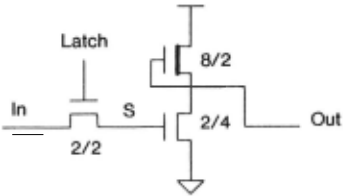
For example, consider an Inverting Latch (Figure 1). This device has two inputs and one bit of state, stored on its S node. The output and next state both depend on the state of Latch. If Latch is high, then Output is not(In) and S is In, otherwise Output is not(S) and S is unaffected. Note that this is a description of its intended digital behavior, and does not refer to signals or voltages.
During verification the following four constraints are posted:
- Latch => overpowers(In, S)
- falls(Latch) => falls-first(Latch ,In)
- control(Latch)
- no-drop(Latch)
The first constraint requires that whenever Latch is true, signal flow must be from In to S. If signal flow is not from In to S, say, because In is a precharged bus and S has more capacitance than In, then the circuit will not have its intended digital behavior. The second con straint requires that if Latch falls during a computation 1 then it can only do so before In changes state. That is , In must either be stable on computations when Latch falls , or, if In is unstable when Latch falls, then In must change after Latch falls. The third constraint requires that once Latch is asserted, it m·ust remain asserted. The fourth constraint requires that Latch not suffer a thresh old drop. Latch is prevented from suffering a threshold drop so that S does not suffer two of them. If any of these constraints are violated, the circuit will not exhibit its intended digital behavior.
3 Relating Multiple Representations of Behavior using Constraints
Circuits have two different levels of behavioral descrip tion: the analog level (also called the signal level), and the digital level. The digital level, which is where the designer designs, is an abstraction of the signal level. This section gives a formal method for relating the two behaviors. This relationship yields the basis for auto matic constraint posting. The next section shows how constraints are posted.
We first introduce notation. Let Design be some struc tural description of a device. Its behavior in some do main D is written BD(Design) . Design's inputs are are written tn = ilD' ... 'inD where lD E Dn. Its out puts are the result of applying its behavior to its inputs: OD = B D (Design)( iD) = o1D, ··· , o.,.,D where OD E DM. Our two domains are sig and dig. We will often leave the domain descriptor off the inputs and outputs and just write i and o. When domain descriptors are elided the sig domain is assumed.
The formal relationship between the signal behavior, B,; 9 (Design), and the digital behavior , Bd; 9 (Design), depends on an abstraction function AB S that maps sig nals into ·digital values . ABS maps signals that don't map into digital values into the error element . .L For mally, ABS : sig => dig+ {1.}. We call any signal for which AB S returns l. invalid, other signals are valid. The following formula gives the formal relationship be tween B ,; 9 (Design) and Bdig (Design).
1 A computation starts when some clock changes state. A computation ends when the circuit reaches state.
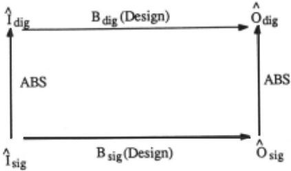
wherever ABS(i) and ABS(Bsig(Design)(t)) are both valid.
This relationship, expressed as a commutative dia gram in Figure 2, says that the digital behavior of a circuit" applied the abstraction of its inputs must be the same as abstracting the result of applying the cir cuit's signal level behavior to its inputs. The key point is that Bdig(Design) does not exist independently of ABS. For example, if ABS returns ..l everywhere, then Bdig(Design) is nowhere defined. A circuit 's digital be havior is defined by the abstraction function used, dif ferent abstraction functions yield different digital behav Iors.
Introducing Constraints
We now extend the above equation include a constraint set C. The constraints will filter out signals that cause either side to yield the error element ..l. Using this con straint set we write the relationship between behaviors as
where the equality must always hold.
The constraint set C has three roles:
- To ensure valid inputs (i.e., that ABS(i) is valid). These are called valid-input constraints and are as sumed to be met .
- To ensure that ABS(Bdig(Design)(t)) is valid. These are called valid-output constraints and can be automatically generated.
- To specialize behavior. These are called logical con straints and must be provided by the designer.
Valid-input constraints are assumed to be met by the environment in which a design operates. Inputs are as sumed to be valid because they either come from the out side world, in which case we must assume they are valid, or they are outputs from other designs, which have their own constraints ensuring their outputs are valid. Only inputs from off-chip must be assumed to be valid, all other inputs are valid because they are outputs of veri fied subcircuits.
Valid-output constraints are automatically generated. Given a representation of ABS(Bdig(Design)(i)) that makes error conditions explicit , constraints are gener ated which ensure the conditions causing the error con ditions never arise. For example, in the signal domain, this how threshold constraints are generated. When an input signal suffering a threshold drop causes an invalid output signal the signal will be constrained from suf fering a threshold drop. The constraint guarantees the output will not be invalid (at least from this particular cause) .
Logical constraints are applied to a circuit's inputs. They specialize circuit behavior and must be provided by the designer . Logical constraints consist mostly of timing information. For example, that two input signals are mutually exclusive, or that a given input signal depends on some other input signal. Logical constraints must be employed when deriving a design's digital behavior from its structure. Otherwise, behaviors which don't arise will be predicted.
4 Automatically Generating Constraints for Combinational Circuits
This section outlines how structure is analysed to yield constraints. The powerful idea is that what must be derived from a design's structure is not its behavior, but the abstraction of that behavior. That is, the important item is not Bsig(Design) , but ABS(Bsig(Design)(i)). As a result, the full actual behavior of Design need not be generated. The focus is generating constraints that ensure that whatever the signal behavior is, it will be abstractable.
Constraint posting occurs in two steps. In the first step, a representation of the signal level behavior of the circuit is created. The representation need not be com pletely detailed. It need only have enough detail so that error conditions can be found. The representation de pends on the abstraction function, it does not contain detail that ABS ignores.
In the second step the abstraction function is applied to the representation to find error conditions which are prevented by the posting of constraints.
As an example, consider a minimally sized inverter.
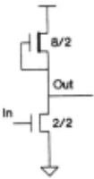
We wish to find the constraints that ensure this device exhibits the digital behavior Ax. not(x). The inverter takes one input signal and yields one output signal.
The abstraction function we use maps a signal into a digital value. If the voltage at the end of the signal is less than 1.5 volts, it returns 0. If the voltage at the end is more than 3.5 volts it returns 1. Otherwise it returns an error indicator. This abstraction function is good enough for combinational circuits, but fails for sequential circuits. Such circuits are discussed in the next section.
The procedure which generates Bsig(Design) from Design knows that AB S only looks at a signal's final value. Therefore it doesn't produce information about the intermediate voltages of the signal. The procedure yields the following the as representation of signal be havior.
Bsig(Inverter) = A in. At. t = t,-+ (voltage(in(t)) = 5-+ 1, 3.5 ~ voltage(in(t)) < 5-+ 1.66, 1.5 ~ voltage(in(t)) < 3.5-+ X, 0 ~ voltage(in(t)) < 1.5-+ 5), Xas the signal behavior of the inverter. This is read as follows . The Inverter takes a signal in and returns a signal, call it out. For any time not equal to t f, the time when the circuit reaches steady state, out returns X, meaning an unknown voltage. When time is t f, out returns a voltage based upon the circuit model and the input voltage.
Applying the abstraction function to the above repre sentation and then simplifying yields
ABS(B,ig(lnverter)) = A in. voltage(in(t,)) = 5-+ false, 3.5 ~ voltage(in(t,)) < 5-+ .l, 1.5 ~ voltage(in(t, )) < 3.5-+ .l, 0 ~ voltage(in(tJ )) < 1.5-+ trueIn is an input and therefore guaranteed to be valid. Therefore the predicate of the third clause will never be true and the class can be deleted. The second clause shows an error condition which arises when the final value of the input signal is between 3.5 and 5 volts. This condition indicates a threshold drop. This error condi tion is prevented by generating the constraint that in cannot suffer a threshold drop.
Deleting these two clauses yields ABS(B,ig(Inverter)) = A in. voltage(in(tJ )) = 5-+ false, 0 ~ voltage(in(tf )) < 1.5-+ true plus the constraint that in cannot suffer a threshold drop.After generating the constraint and getting to this point, further transformations and rules are used to prove that the circuit exhibits the digital behavior A x . not( x). These transformations are outside the scope of this paper.
5 Generating Constraints for Sequential Circuits
We verify circuits with state the same way we verify corn binational circuits. We apply an appropriate abstraction function to the outputs of the circuit and generate con straints to eliminate .l wherever it appears. Signals at nodes storing state are also considered to be outputs of the circuit: they must also abstract to digital values. The abstraction used for combinational circuits, which looks only at the final values of signals, projects an in adequate digital behavior for circuits with state. Unlike combinational circuits , whose outputs can be predicted solely from the final values oftheir input signals, the out puts of circuits with state depends on the circuit's entire input waveforms and internal waveforms. We need new constraint types to control the types of waveforms pre sented to, and generated by, a circuit.
We want the abstraction function to be able to predict a circuit's outputs and next state solely from the circuit 's initial state and the final values of its input signals . This requirement abstracts away the detailed behavior of each signal. To meet this requirement we prevent charging or discharging of capacitors that can not be predicted from the circuit's initial state and· the final values of its input signals. We say that the charge at a node (capacitor) has been corrupted when the capacitor unpredictably charges or discharges. A signal at such a node is also called corrupted.
To prevent the corruption of stored charge the in ternal events of a computation are ordered by us ing two timing constraints: stable-after(Sl,S2) and falls-first(Sl,S2). Signal S2 is stable after signal Sl when S2's voltage does not change after Sl is as serted. The constraint control(Sl) is shorthand for stable-after(Sl,Sl). Signal Sl falls before signal S2 if Sl falls before S2's voltage changes. These are the only constraints needed to ensure stored charge is not corrupted.
The signals of nodes which do not store state, do not gate transistors, and which are not outputs of circuits are not abstracted. Such nodes, called connection nodes, serve only as vias for information flow. Because con nection nodes are never abstracted, the signals at those nodes are irrelevant. Nodes that store state are found by a simple static recursive tree walk starting from a circuit's outputs [Weise, 1986].
5.1 The New Abstraction Function
We introduce new nomenclature and concepts before presenting the abstraction function. Signals that come from off chip (e.g., Vdd and GND) are driven. Signals that come from capacitors are undriven. A node is driven at some time t if it is connected at time t through zero more conducting transistors to a driven signal, otherwise it is undriven.
The final voltage of a signal must be predictable from the initial state of the circuit and the final values of the circuit's inputs. There are two cases to consider: when a signal is driven at steady state, and when it is undriven at steady state. When it is driven at steady state its final voltage is computed using the methods as for com binational circuits. When it is undriven at steady state we require that at steady state it must be connected to any nodes it was connected to during the computation. When this requirement is met , the charge on the node can be computed from its initial charge and the initial charges of nodes it is connected to when the computation ends.
We augment signals to include strength. Where signals used to map time into a voltage, they now map time into a voltage and a strength. We define the strength of a signal at node Nat timet as the sum of the capacitances of the nodes N is connected to at time t. Off-chip inputs are considered to have infinite capacitance. The strength of a signal at a node indicates what happens to the node over time. Strength that increases over time indicates that the node is sharing charge with increasing numbers of nodes. Strength that decreases over time indicates that the node is sharing charge with fewer nodes over time.
One seemingly obvious rule to ensure that a circuit's final state can be predicted from its initial state and the final state of its inputs is to require that a signal's strength cannot decrease after increasing. This rule is not strict enough. It won't catch the case where an infi nite strength signal changes its voltage without changing its strength.
A simple change on the above rule does the trick. Let STB {Signal To Boolean) be the abstraction function used previously for combinational circuits. The new ab straction function is: "If signal S's strength decreases after its voltage changes then .l, else STB{S). 2 This new abstraction function maps any signal that represents cor rupted charge into .l. We now discuss timing constraints for preventing non-digital signals.
5.2 Generating Timing Constraints
The generation of timing constraints is a new step that does not materially affect how signal behavior is gener ated or represented. Although Silica Pithecus produces timing constraints directly from the signal behavior rep resentation, for expository reasons we present the gen eration of timing constraints in terms of net transition graphs, which are a pictorial representation of signal be havior . This section first describes net transition graphs, then gives the rules for generating timing constraints from net transition graphs .
A net transition graph is built for every node that might be undriven at steady state. The graph has a vertex for every clause of the node's signal behavior rep resentation, i.e., for each net the node might be a mem ber of during a computation. The vertex includes the strength of the net and the condition when the net oc curs. The information in the net transition graph that isn't in the net behavior is the information in its edges. If net N1 can become net N2 when transistor T changes state then there is a directed edge , labeled by the tran sition, from the vertex for N 1 to the vertex for N2. An edge, or transition, is called downwards when the strength of N1 is greater than the strength of N2. Up wards and sideways edges are defined similarly.
2 The real abstraction function is slightly more compli cated than this, as the "drivenness" of a signal is preserved by the abstraction function . The real abstraction function maps signals into seven values: driven 1, driven 0, floating 1, floating 0, driven 1., floating 1., and 1. .
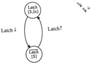
For example, consider the net transition graph of the Inverting Latch 's S node {Figure 3). This has two nodes, one for the net [S], which occurs when Latch is false, and one for net [S, In) , which occurs when Latch is true. There are two edges , an upwards one for Latch going from false to true, and a downwards one for it going from true to false.
Silica Pithecus generates timing constraints directly from a node's net transition graph. The three rules listed below are applied at each vertex. These rules ensure strength doesn't decrease after voltage changes. The first two rules are enforced by stable-after constraints. The third rule is enforced by falls-first constraints.
- A downward transition cannot follow an upward transition.
- A downward transition cannot follow a sidewards transition between vertices of infinite strength.
- A downward transition from net N cannot occur af ter an input / output node in net N changes.
For example, consider again the net transition graph of the Inverting Latch's S node {Figure 3) . No rules trigger for the lower vertex, but two rules, 1 and 3, trigger for the upper vertex. These two rules create the following constraints.
- control{Latch,) = stable-after{Latch, ,Latch,)
- falls{Latch,) ::} falls-first{ Latch, ,In,)
6 Hierarchical Verification
Hierarchical verification first processes the constraints of each subcircuit. If no constraint is violated, then the digital behavior of the whole is derived from the digital behaviors of the subcircuits.
Our constraint processing is similiar in Spirit to Mol gen's, but there are two major differences. First, because we are performing analysis and not synthesis, the satis faction of a constraint does not cause new processing to take place. Second, because our constraints have very specific meanings, our constraint processing is principled rather than ad hoc, as it is in Molgen.
There are three possible outcomes from processing constraints: a constraint can be accepted, rejected, or propagated. A constraint is accepted when it is shown to hold. A constraint is rejected when is is proven not to hold. Rejected constraints represent design errors and are reported to the designer. When there is not enough information to show that a constraint either holds or doesn't hold, the constraint is propagated up the struc tural hierarchy to be reprocessed when the circuit itself is used as a subcircuit. As in Molgen, constraints can change form when they are propagated. For example, when a component of circuit C requires that X falls be fore Y, this may only be met if Q falls before X in circuit C. This new condition is the constraint thet is propa gated.
There are dedicated handlers for each type of con straint . The information needed to process a constraint is constraint dependent. Logical constraints are handled by a simple tautology checker. Threshold constraints are handled by a marking scheme. Timing constraints are handled by proving mutual exclusion among signals. All the constraint handlers are conservative. When they are unable to prove a constraint holds, they report it doesn't hold.
As a concrete example of hierarchical verification, con sider a Shift Cell built out of two juxtaposed Inverting Latches.
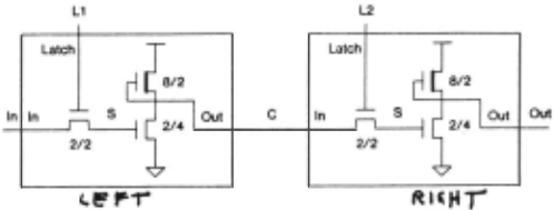
The Shift-Cell takes two inputs and its behavior is equivalent to two inverting latches, one feeding the other. There is one logical constraint for the shift cell which declares that L1 and L2 are mutually exclusive.
When given the above information, Silica Pithecus de clares the Shift Cell to be correct and propagates the following six constraints:
- L1 => overpowers([In] , [(S Left)])
- control(L1)
- control(L2)
- no-drop(L1)
- no-drop(L2)
- falls(L1) => falls-first(L1, In)
These constraints result from propagating the six un resolved constraints from the two Inverting Latches to the Shift Cell. In total , eight constraints were generated for the Shift Cell, but only two were satisfied:
- L2 => overpowers([C],[(S Right)]) and
- falls(L2) ---+ falls-first(L2 , C) .
7 Conclusions
We have successfully applied constraint posting to the problem of VLSI circuit verification. Silica Pithecus is implemented on Symbolics 3600's. It verifies complex circuits containing about 1000 transistor in one minute. Less complex circuits with equivalent numbers of tran sistors are verified much more rapidly. Not all the con straint checkers are fully implemented, so these timings are slightly better than they should be were all checkers implemented.
Our methods relied on a formal method for relating a circuits signal and digital behaviors. This method al lowed us to automatically post constraints for a large class of circuits .
These ideas can also be used in a circuit synthesizer. I envision a circuit synthesizer which operates along the same lines as Molgen. It makes decisions and posts con straints to constrain other decisions.
The automatic generation of constraints can be used in any domain where the relationship between behavioral representations can be formalized.
@inproceedings{ijcai1989p141,
  title     = {Constraint Posting for Verifying VLSI Circuits},
  author    = {Weise, Daniel},
  booktitle = {Proceedings of the Eleventh International Joint Conference on
               Artificial Intelligence, {IJCAI-89}},
  publisher = {International Joint Conferences on Artificial Intelligence},
  editor    = {N. S. Sridharan},
  pages     = {881--885},
  year      = {1989},
  month     = {8},
  note      = {Planning, Scheduling, Reasoning About Actions},
  url       = {https://ijcai.org/proceedings/1989/141},
}
TY - CPAPER TI - Constraint Posting for Verifying VLSI Circuits AU - Weise, Daniel T2 - Proceedings of the Eleventh International Joint Conference on Artificial Intelligence, IJCAI-89 PB - International Joint Conferences on Artificial Intelligence PY - 1989 SP - 881 EP - 885 UR - https://ijcai.org/proceedings/1989/141 ER -Copied
Machine-readable versions of this paper, for tools and AI agents: